|
LAB ON A CHIP Please use our A-Z INDEX to navigate this site where page links may lead to external sites ABOUT - CIRCUMNAVIGATION - CLIMATE CHANGE - CONTACTS - DONATE - FOUNDATION - OCEAN CLEANUP - HOME - A-Z INDEX
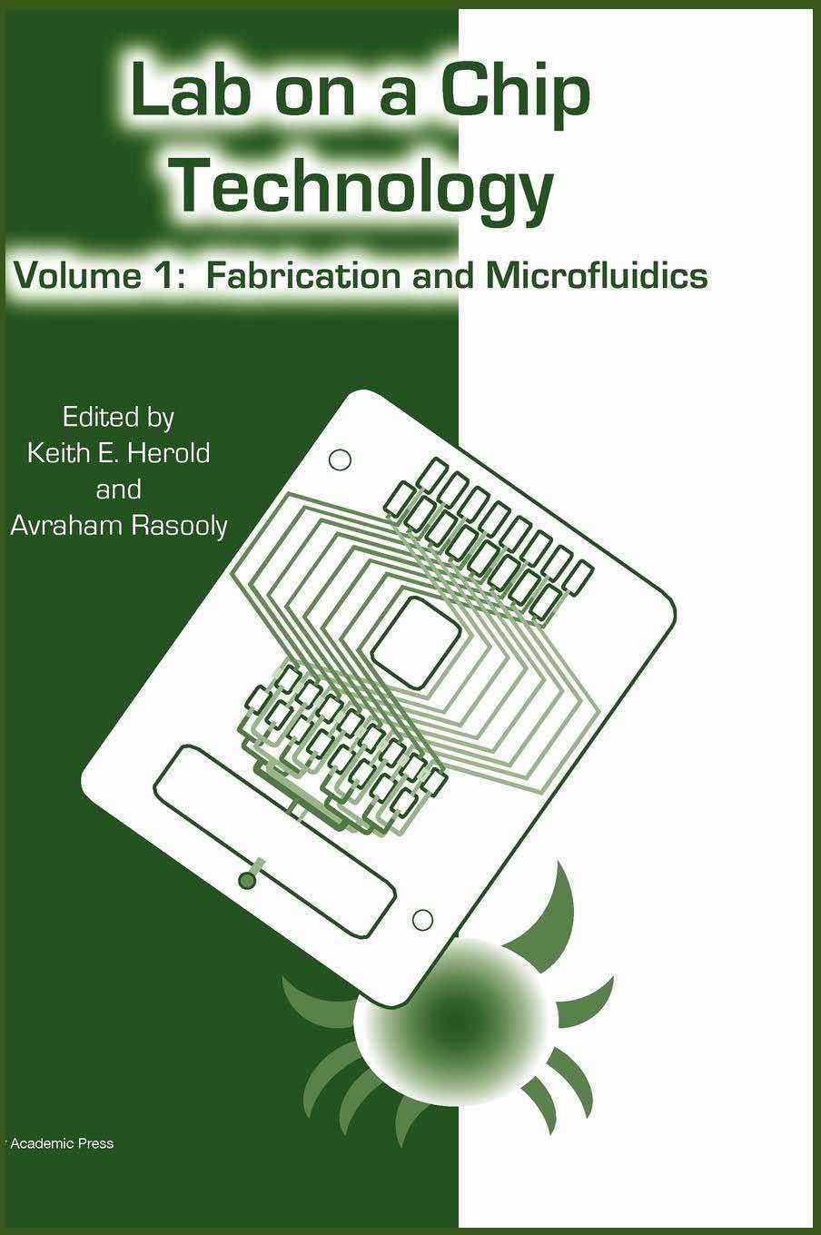
An advanced Lab On A Chip design. The technology is out there, just waiting to be adapted to various purposes.
Electronics and computer programs can achieve in seconds what human scientists might take several hours to complete. Not only that, but monitoring and analysis can be continuous. This is ideal for use by SeaVax for monitoring the state of the oceans, cost effectively. Such a system could also be used to combat Covid19 and monitor the state of human health generally.
WHAT IS A LAB ON A CHIP? A Lab-On-a-Chip (LOC) is a device that integrates one or several laboratory functions on a single integrated circuit (commonly called a "chip") of only millimeters to a few square centimeters to achieve automation and high-throughput screening.
LOCs can handle extremely small fluid volumes down to less than pico-liters. Lab-on-a-chip devices are a subset of Micro Electro-Mechanical Systems (MEMS) devices and sometimes called "micro total analysis systems" (µTAS). LOCs may use microfluidics, the physics, manipulation and study of minute amounts of fluids. However, strictly regarded "lab-on-a-chip" indicates generally the scaling of single or multiple lab processes down to chip-format, whereas "µTAS" is dedicated to the integration of the total sequence of lab processes to perform chemical analysis.
The term "lab-on-a-chip" was introduced when it turned out that µTAS technologies could be applied to more than analysis only purposes.
PHYSICS.ORG FEB 24 2015
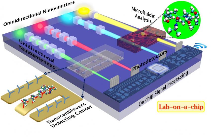
The new cubic nanoantennas have the potential to revolutionize the infant field of nano-electromechanical systems (NEMS). "These unidirectional nanoantennas are most suitable for integrated optics-based biosensors to detect proteins, DNA, antibodies, enzymes, etc., in truly portable lab-on-a-chip platforms of the future," Sikdar said. "They can also potentially replace the lossy on-chip IC (integrated circuit) interconnects, via transmitting optical signals within and among ICs, to ensure ultrafast data processing while minimizing device heating," he added.
ABSTRACT
Lab-on-a-Chip Technology (Vol. 1): Fabrication and Microfluidics
"a comprehensive and felicitous compendium" (Drug Research)
Publisher: Caister Academic Press
Edited by: Keith E. Herold (1) and Avraham Rasooly (2)
"a comprehensive view on state of the art LOC technologies ... Overall the double volume represents a comprehensive and felicitous compendium of lab-on-a-chip technologies and applications not only for the beginner going to get started development experimentally in a fast growing and innovative technology. But also the skilled specialist staying in the commercial arena might find a hugely satisfying compilation of state of the art LOC technologies and new ideas for sure ... All in all 'Lab-on-a-Chip Technology' is a very useful reading for everyone who is interested in development and production of LOC devices." from Arzneimittel-Forschung/Drug Research (2009) 59: 672-673.
1. Introduction to Microfluidics
Keith Herold and Avraham Rasooly
This short overview discusses the fundamental elements of moving fluids in lab-on-a-chip (LOC) systems. Liquid flow in such systems is usually either single-phase channel flow or droplet flow on a surface (or between two surfaces). A primary characteristic of all flows considered here is that they are laminar flows, which provide a series of benefits as well as some challenges. Some of such basic elements described in this chapter are channel flows, pressure driven flow, electroosmotic driven flow, capillary effects, surface forces, mixing and two-phase flow.
2. Fabricating PDMS Microfluidic Channels Using a Vinyl Sign Plotter
Michael Armani, Roland Probst and Benjamin Shapiro
A novel technique is presented for creating PDMS microchannels from molds produced by a sign plotter, which can be done quickly, cheaply, and in-house. To do this a vinyl template is made using a sign plotter, a negative template is made from the vinyl using an epoxy mold, and a final PDMS mold is made using the epoxy template. This method allows for microchannel design and fabrication in less than 2 hr, without the need for clean room lithography or a chrome mask, and eliminates the poor transparency, poor sealing, and adhesive residues of microchannels made directly from vinyl cutouts. This fabrication process was used to create channels to demonstrate microfluidic flow control of particles.
3. Functionalized Glass Coating for PDMS Microfluidic Devices
Adam R. Abate, Daeyeon Lee, Christian Holtze, Amber Krummel, Thao Do and David A. Weitz
Microfluidic devices can perform multiple laboratory functions on a single, compact, and fully integrated chip. However, fabrication of microfluidic devices is difficult, and current methods, such as glass-etching or soft-lithography in PDMS, are either expensive or yield devices with poor chemical robustness. We introduce a simple method that combines the simple fabrication of PDMS with superior robustness and control of glass. We coat PDMS channels with a functionalized glass layer. The glass coating greatly increases the chemical robustness of the PDMS devices. As a demonstration, we produce emulsions in coated channels using organic solvents. The glass coating also enables surface properties to be spatially controlled. As a demonstration of this control, we spatially pattern the wettability of coated PDMS channels and use the devices to produce double emulsions with fluorocarbon oil.
4. Fabrication of Lab-on-a-Chip Devices Using Microscale Plasma Activated Templating (μPLAT)
Robert Carlson, Shih-hui Chao and John Koschwanez
This chapter presents an integrated package of techniques, microscale PLasma Activated Templating (μPLAT), that enable rapid bench-top microfabrication. μPLAT can be used to quickly fabricate low-cost lab-on-a-chip devices that contain features that are difficult to achieve using photolithography-based methods. For applications with resolution requirements above 50 μm, functioning devices can be made without the use of cleanroom operations, photolithography, and intensive chemistry. We present devices fabricated using μPLAT that contain components for on-chip heating, temperature measurement, pumping, and single-cell level trapping.
5. Bonding Techniques for Thermoplastic Microfluidics
Chia-Wen Tsao and Don L. DeVoe
The use of thermoplastic polymers as microfluidic substrates is a robust and growing area of research, with important implications for the development of low cost disposable microfluidic devices for a host of bioanalytical applications. Substrate bonding is a critical step required for the formation of sealed microchannels within thermoplastic chips. Unlike silicon and glass, the diverse material properties of thermoplastics opens the door to an extensive array of substrate bonding options, together with a set of unique challenges which must be addressed to achieve optimal sealing results. This chapter reviews the range of techniques developed for sealing thermoplastic microfluidics. In addition to summarizing and discussing practical issues surrounding these various bonding methods, detailed process descriptions for selected sealing techniques are provided.
6. Xurography: Microfluidic Prototyping with a Cutting Plotter
Daniel A. Bartholomeusz, Ronald W. Boutté and Bruce K. Gale
Prototyping is necessary to show proof-of-concept for microfluidic applications and to develop and optimize functional microfluidic features unique to each LOC application. Each microfluidic feature depends on the application's chemistry, sample, purpose, detection method, and desired functionality. Inexpensive and rapid prototyping will accelerate the product-to-market and results-to-publication, whether you are developing a novel Lab-on-a-Chip (LOC) for a particular application or using a previously developed LOC technology to test the feasibility of a particular assay.
This chapter discusses a rapid and inexpensive micro-fabrication technique using a cutting plotter (a plotter fit with a knife blade) with 10 μm resolution, to directly cut microstructures in thin polymer films that can be laminated into complete microfluidic devices, without photolithographic processes or chemicals. Cutting plotters are ideal for microfluidic prototyping because they can cut micro-features with aspect ratios of 1 - 2 times the material thickness in films ranging from 25 - 1000 μm thick. The plotters also costs less that ,000 and materials cost much less than a photomask. Multi-layered microfluidic structures cut from pressure sensitive and thermal activated adhesive films can be cut and laminated in less than 30 minutes. This method of using a cutting plotter to prototype is called Xurography, for the Greek root words Xuron and graphe meaning razor and writing, respectively. This inexpensive method can rapidly build microfluidic devices or tertiary fluid connections for higher resolution devices.
Edwin T. Carlen, Johan Bomer, Jan van Nieuwkasteele and Albert van den Berg
The past two decades have seen rapid advancement of Lab on a Chip (LOC) systems with applications ranging from gas chromatography to capillary electrophoresis, and more recently to high-pressure chemistry and single cell analysis. For many applications in clinical medicine, biology and chemistry, silicon and glass may still be the preferred materials. The mechanical rigidity, chemical resistance, and low permeability properties of silicon and glass, combined with the optical transparency of glass, make them a good choice for many demanding LOC applications. The large and well developed silicon and glass micromachining toolbox provide the capability to obtain microstructures with high precision and repeatability. In addition, scaling device dimensions down to the nanometer scale is relatively straight forward using silicon and glass micromachining, which is important for emerging fields, such nanofluidics and nanosensing.
8. Flow Lithography for Fabrication of Multi-Component Biocompatible Microstructures
Yuk Kee Cheung, David Shiovtiz and Samuel K. Sia
This chapter details and expands upon the original flow lithography procedure that we have developed to directly pattern multi-component microstructures made up of biocompatible hydrogel. We discuss in detail the relevant experimental parameters for making the fabrication technique work in practice as well as the parameters needed to render the substrates compatible with mammalian cells.
9. Microtechnology to Fabricate Lab-on-a-Chip for Biology Applications
Sang-Hoon Lee
Recently, basic experimental techniques and associated equipments and tools in a biology laboratory are changing to handle small quantities of samples more efficiently and 'Lab on a chip (LOC)' is one of the latest emerging technologies. To satisfy the diverse requirements of biologists rapidly, it is recommendable for biologists themselves to design and fabricate LOC; however, it is still difficult for them to start. This chapter is written to introduce the overview of microfabrication technology for LOC and the practical method for fabricating LOCs with three examples.
10. Cyclic Olefin Copolymer (COC) Polymer Molding for LOC
Dong Sung Kim and Kwang W. Oh
Cyclic olefin copolymer (COC) draws attention as a primary substrate material for the microfluidic lab on a chip (LOC) applications based on its various advantages with regards to physical and chemical properties. For the replication of small structures (especially less than 10 μm), hot embossing is preferable and provides the simple fabrication process compared to the injection molding technique. However, as far as productivity is concerned, an injection molding process is the most effective replication technique for the polymer based LOC which has microstructures with feature size greater than 10 μm. In this chapter, (i) the fabrication process of silicon and polydimethylsiloxane (PDMS) mold inserts and the hot embossing process, and (ii) the proper processing windows of the injection molding and thermal bonding processes of the COC microfluidic LOC are described and discussed in detail. For the injection molding of the COC LOC, the fabrication process of nickel mold inserts is introduced based on UV-photolithography and subsequent electroplating process. A mold base which enables us to utilize a number of fabricated mold inserts by simple replacement is described to develop various types of injection molded COC LOC. Materials required for the whole fabrication process of the COC microfluidic LOC are also provided. Finally, application examples of the molded COC LOC and the perspective on future trends of the COC polymer molding process are provided.
11. Laminated Object Manufacturing (LOM) Technology Based Multi-Channel Lab-on-a-Chip for Enzymatic and Chemical Analysis
Steven Sun, Nikolay Sergeev, Jesse Francis, Yordan Kostov, Minghui Yang, Hugh A. Bruck, Keith E. Herold and Avraham Rasooly
Lab-on-a-chip (LOC) technology has the potential to greatly simplify analytical analysis by providing a platform for chemical and biochemical reactions as well as the analysis of such reactions without a laboratory. Prototyping of LOC is critical for rapid and low cost system development. Among the many prototyping methods, Laminated Object Manufacturing (LOM) technology is one of the most rapid and cost effective options. Using this method, it is possible to create 3D microfluidic structures by assembling a stack of polymer sheets, where each layer is fabricated by laser machining of a polymer sheet such as acrylic or polycarbonate and bonding the layers with adhesive. The main elements of LOM using polymer sheets are described here, including LOC design, laser machining, bonding and testing. An example of an eight channel LOC for enzymatic and chemical analysis based on mixing two reagents is provided. The technology, combined with suitable medical assays, has the potential to enhance the quality of health care and to provide care to underserved populations.
12. Laser Micromachining
Emanuel Waddell
The use of microfluidic devices is making rapid inroads in the modern analytical laboratory, primarily because of their small physical footprint, speed and efficiency of chemical separations, and reduced reagent consumption. Traditionally, lab-on-a-chip devices have been manufactured in silica due to its well understood surface chemistry and favorable micromachining techniques that are ubiquitous in the microelectronics industry. These techniques are typically based on silica etching which is time consuming, requires specialized resources, and utilizes a large amount of chemical solvents that pose unique safety and environmental hazards. Recently researchers have begun to utilize devices fabricated from polymer substrates as an alternative to glass. Reasons include reducing the total cost and the ability to tailor physical and chemical properties which may include surface roughness, surface charge, optical clarity, and tensile strength. For example, polymer substrates typically have greater impact resistance than glass and when one considers mass production, the cost of polymer substrates are a fraction of the cost of glass which leads to a large amount of savings. However, some of the advantages of using polymers are negated by the traditional microfabrication techniques used to manufacture metal or silicon molds which are subsequently utilized to fabricate polymer devices by imprinting or injection molding. The primary negative associated with manufacturing molds in the laboratory by traditional methods is the time commitment for the production of the original mold and the inability to modify the mold. This proves to be costly and time consuming. In a research and development environment it is important that researchers have access to fabrication techniques that are rapid and easily implemented with a variety of substrates. In addition it is important that changes in the fluidic circuit be implemented with minimal cost and limited time investment. Laser micromachining has been proven to be such a technique and this brief discussion describes the fabrication of simple fluidic circuits in a polymer substrate. In summary, this chapter will examine the practical details involved in laser micromachining provided from the perspective of the novice researcher who desires to utilize the technique for scribing simple microfluidic circuits in readily available polymer substrates.
13. Shrinky-Dink Microfluidics
Anthony A. Grimes, Brent D. Rich, Maureen Long, Diep Nguyen and Michelle Khine
Fabricating small and intricate patterns into silicon, glass, or quartz is traditionally expensive as well as manually and time intensive. These setups typically require investments in large specialized equipment, a cleanroom, and costly consumables. To translate from academic prototyping in engineering labs to truly useful analytical tools for researchers from the range of fields that "Lab on a Chip" technologies is predicted to eventually benefit, this field must mature to the point where robust and specifically designed devices can be readily realized. Ideally, researchers can conceive of a specific device design that can uniquely help investigate their hypothesis-driven investigation, and then within minutes, have in their hands a fully functional device. We have recently developed a new technique to circumvent the time and expense of conventional photolithography by leveraging the inherent shrinkage properties of the child's toy Shrinky-Dinks. Shrinky-Dinks are sheets of pre-stressed polystyrene (PS) sheets. By simply patterning these polystyrene sheets, we can create microfabricated patterns. The process we have developed is even faster than soft lithography, the commonly accepted prototyping standard for microfluidics. Furthermore, this technique obviates the high-tooling and consumable costs of photolithography altogether. Using this technique, 3D chips can even be rapidly developed directly in polystyrene (PS). In this review, we characterize the shrinkage performance of these thermoplastics and the tolerances of the patterning. While the tolerances achievable with this thermoplastic cannot yet compete with photolithography, they are sufficient for many applications. In fact, certain applications particularly benefit from the inherent channel geometries (e.g. rounded channels) that result from this approach. We demonstrate how to make and use such devices in this chapter.
Section II. Fluid Control and Manipulation
14. Simple Recipe for Electroosmotic Mixing in Microchannels
Nadine Aubry
Efficient mixing is often a crucial step in Lab on a Chip (LOC) devices. Yet, it has been difficult to achieve as flows in such devices are typically laminar and thus one cannot count on turbulence as a mixing mechanism in these flows. While most solutions proposed so far require the alteration of the device geometry, or the addition of electrodes in the channel walls, in this chapter we concentrate on inducing mixing in electroosmotic flow simply by using the electrodes already in place for flow pumping, as previously proposed in earlier work. The microchannel consists of two inlets and one outlet in order to bring the two liquids together. The heart of the technique lies in the modification of the voltages applied to the inlet electrodes. We recall that good mixing is obtained when the electroosmotic flow at the two inlets is pulsed out of phase, the phase difference is 90 degrees rather than 180 degrees, and the pulse volume is comparable to the intersection volume. While the technique is not new, the goal of this chapter is to present the steps needed in the form of a ready-to-use recipe, as well as provide additional details.
15. Electrowetting-on-Dielectric (EWOD) Microfluidic Devices
Sang Kug Chung, Yuejun Zhao and Sung Kwon Cho
Since the emergence of microfabrication technology, microfluidics has bloomed, bringing a revolutionary concept: lab on a chip which is currently having tremendous impact in biomedical applications. In particular, droplet-based digital microfluidics, in which fluids are handled in a droplet form rather than continuous streams in microchannels, has developed as a new paradigm and is growing in popularity alongside conventional microchannel-based microfluidics. Electrowetting on dielectric (EWOD), which enables efficient manipulation of droplets, is greatly contributing to the development, maturation, and realization of digital microfluidics. This chapter begins with a brief description and discussion on EWOD principle and background. Then, detailed design and fabrication technology of simplified EWOD testing chips with dual plane driving scheme are described with emphasis on hands-on microfabrication process. In addition, as fundamental operations of droplets and bubbles, it is demonstrated how to manipulate (transport and split) droplets and bubbles using the testing chips. Finally, it is shown that transportation of droplets and bubbles is immediately applied to collection and manipulation of microparticles, respectively. It is expected that the present EWOD configuration would serve as a template that can be easily adopted for the real-world lab-on-a-chip applications.
16. Introduction to Electrokinetic Transport in Microfluidic System
In this chapter we provide an introduction to the use of electrokinetic transport in lab-on-chip devices and other microfluidic systems. Specifically we focus on direct current (DC) electrokinetic phenomena (electroosmosis, electrophoresis and dielectrophoresis) and its use in transporting a range of different species from biomolecules to cells. In the first part of this chapter we introduce a simple theoretical framework for electrokinetic transport. Sufficient detail is provided to describe the underlying physics without requiring overwhelming mathematics. This is followed by detailed description of a simple experimental implementation of electrokinetics for DNA hybridization analysis. The effects of transport on the hybridization efficiency are discussed along with methods by which numerical analysis can help design optimal chip operational conditions. In the final section the advantages and disadvantages of electrokinetics are discussed in the context of other methods of performing on-chip transport and some future analytical needs.
17. Frequency and Polarity Effects of Droplet-based LOC Driven by Electrowetting
Shih-Kang Fan
Electrowetting has been extensively studied and applied as a pumping mechanism in droplet-based Lab-on-a-Chip (LOC). The electrically controllable liquid-solid contact angle is proportional to the square of the applied voltage and described by the Lippmann-Young equation. Thus, the frequency and polarity effects are easily ignored. In this chapter, the basic electrowetting phenomenon is introduced. Two basic types of electrowetting-based LOC, including sandwiched and open devices, are presented. Moreover, the frequency effect is applied to realize a particle concentrator in a sandwiched device, while the polarity effect is employed to manipulate droplets by a square wave signal on an open device. In the frequency effect study, the applied low frequency signals are consumed mostly in the dielectric layer and cause electrowetting to pump liquid droplets on the millimeter scale. High frequency signals establish electric fields in the liquid and generate dielectrophoresis forces to actuate cells or particles on the micrometer scale inside the droplet. In the polarity effect study, electrowetting on an SU-8 and Teflon coated electrode is investigated. It is found that the Θ-V (contact angle-applied voltage) curve is asymmetric along the V = 0 axis by sessile drop and coplanar electrode experiments. A systematic deviation of measured contact angles from the theoretical ones is observed when the electrode beneath the droplet is negatively biased. In the sessile drop experiment, up to a 10 degrees increment of contact angle is measured on a negatively biased electrode. Asymmetric electrowetting is then applied to oscillate and transport droplets on square-wave-powered symmetric (square) and asymmetric (polygon) coplanar electrodes to demonstrate the manipulation capability of an open device.
18. Linear Dilution Microfluidic Devices
Adrian T. O'Neill and Glenn M. Walker
Linear dilution is a method to create linearly varying concentrations of a solution. Linear dilutions are commonly used in biological studies where the threshold concentration at which a physiological reaction occurs is unknown, whether it be a minimum effective or a maximum tolerable dosage. In this chapter we present a summary of the approaches used for creating dilutions with microfluidics followed by a detailed methodology for constructing a proportional mixing linear dilution microfluidic device. The microfluidic device presented here is made with a rapid and inexpensive microfabrication method, soft lithography. The device is capable of generating nine linearly varying dilution values with an R2 value exceeding 0.999 and the linearity of the dilutions is independent of the input flowrate, making it a very robust approach to creating linear dilutions. With the model presented the device can be expanded to an arbitrary number of dilutions with commensurate savings in reagent usage and time.
19. Monolithic Membrane Valves and Pumps
William H. Grover and Richard A. Mathies
Since their initial description in 2003, monolithic membrane valves and pumps have found uses in lab-on-a-chip devices for a variety of different applications. These valves and pumps offer a variety of advantages over conventional "soft lithography" structures, including improved assay compatibility, resistance to virtually all chemicals, and the ability to control device operation using on-chip valve-based logical circuits. In this chapter we introduce monolithic membrane valves and pumps in Section 1. We then present a detailed description of the materials and methods used to fabricate devices containing monolithic membrane valves and pumps in Sections 2 and 3. Using these methods, researchers have fabricated lab-on-a-chip devices for a great variety of different applications, and we examine several of these applications in detail in Section 4. Finally, prospects for future monolithic membrane valve- and pump-based devices are considered in Section 5.
20. An Active Micromixer Based on Non-equilibrium Electrokinetics for Lab-on-a-Chip Systems
Daejoong Kim
This chapter describes a new type of micro/nano fluidic mixer based on non-equilibrium electrokinetics. The device is fabricated with two-step reactive ion etching, one for nanochannels and one for microchannels. Mixing is achieved by strong vortex structures formed near the micro/nano channel interface. The micro/nano fluidic mixer is expected to be beneficial in the development of many lab-on-a-chip systems, since it is simple in its design with minimal fabrication complications.
21. Surface-Machined Parylene Microfluidics
Jason Shih, Terry D. Lee and Yu-Chong Tai
Over the last decade we have pioneered a unique technology for the realization of microfluidic components and systems. The technology is based around Parylene, a thin film, chemically inert, and biocompatible polymer deposited using a room temperature chemical vapor deposition (CVD) process. Surface micromachining, a common technique in microfabrication, is used to build up our fluidic structures one Parylene layer at a time. Using this technology, a portfolio of microfluidic components, ranging from pumps and valves, to flow and pressure sensors, have been demonstrated. Since all these components are produced using the same technology, the total integration of different components to form a system is feasible. The use of Parylene also ensures that the final microfluidic devices are biocompatible and chemically resistant to a broad range of solvents. Finally the use of microfabrication techniques allows us to batch fabricate devices simultaneously.
Beyond the core Parylene surface micromachining technology, we have also developed additional methods to adapt our technology for different specific needs. These include the modification of the core technology to produce fluidic structures capable of sustaining pressures greater than 1000 psi for applications such as high performance liquid chromatography (HPLC). Also, we have demonstrated a modular concept where chips with different components can be connected together on a microfluidic breadboard.
Ronalee Lo and Ellis Meng
Emerging lab-on-a-chip systems have rapidly advanced the field of microfluidic systems for use in biological and chemical applications. These systems require carefully designed packaging to reliably connect microfabricated fluidic channels to macro-world interfaces. Macro-to-micro fluidic interfaces, unlike their electrical analogues, is still an active area of research and despite many efforts, a suitable standard does not exist. A review of current macro-to-micro fluidic interface technologies is presented. Then several practical macro-to-micro interface methods are described in detail along with step-by-step protocols for their construction and implementation. These connections described were selected for their compatibility with most microfluidic system layouts, materials, and system requirements.
A review with 64 references that describes and gives experimental details for the injection modes commonly used in microchip-based electrophoresis and flow injection analysis. The two most frequently used electrokinetic injection techniques, pinched and gated injection, are first reviewed. In the context of electrokinetic injections, a description on how the detection mode can influence the method of injection is given, as detection modes such as electrochemistry have the requirement that no potential can be applied to the reservoir where the electrodes reside. Additionally, work we have published using elastomeric valves to couple hydrodynamic injections to microchip electrophoresis is detailed. Finally, the methods that can be used to perform reproducible and discrete injections for microchip-based flow injection analysis are discussed.
The importance given to innovation saw significant differences between countries and industries: Germany, Ireland and Italy, countries where there is a clear government drive for innovation together with a well-established start-up and entrepreneurial culture, have it high on the agenda, and unsurprisingly, innovation also features heavily on the boardroom agenda of life sciences and TMT industries, but less so in construction and energy and resources. Product innovation was the area receiving the most attention.
LINKS & REFERENCE
https://www.caister.com/loc1 https://pubs.rsc.org/en/content/articlelanding/2011/lc/c1lc20144a/unauth#!divAbstract https://www.mdpi.com/2076-3905/4/4/570 https://phys.org/news/2015-02-optical-nanoantennas-stage-nems-lab-on-a-chip.html
MARINE LIFE - This humpback whale is one example of a magnificent animal that is at the mercy of human activity. Humans are for the most part unaware of the harm their fast-lane lifestyles are causing. We aim to change that by doing all we can to promote ocean literacy.
This website is provided on a free basis as a public information service. Copyright © Cleaner Oceans Foundation Ltd (COFL) (Company No: 4674774) 2020. Solar Studios, BN271RF, United Kingdom. COFL is a charity without share capital. The names Amphimax™ RiverVax™ and SeaVax™ are trademarks.
|